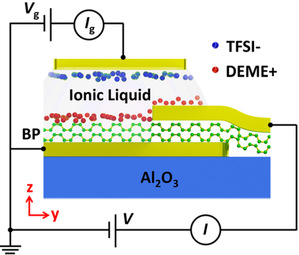
We report on a novel realization of few-layer black phosphorus (BP)-based vertical JoFETs using an electric-double-layer configuration. In transport experiments, using junctions of different shape, superconducting quantum interference device-like magnetic diffraction patterns of the junction critical current and anomalous Shapiro steps on current voltage characteristics are observed, strongly indicating that the critical current density in the junctions is highly inhomogeneous and peaked at the edges or even near the junction corners. The electric-field tunability of the Josephson coupling could be attributed to the edge- or corner-dominated supercurrent density profile combining with the carrier diffusivity in the few-layer BP. The ability to control the vertical Josephson coupling provides us with new opportunities to study high-performance and high-temperature superconducting Josephson field-effect transistors operating on an atomic-scale channel length.
Appl. Phys. Lett. 119, 072601 (2021) |
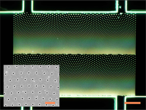
We demonstrate a superconducting diode achieved in a conventional superconducting film patterned with a conformal array of nanoscale holes, which breaks the spatial inversion symmetry. We showcase the superconducting diode effect through switchable and reversible rectification signals, which can be three orders of magnitude larger than that from a flux-quantum diode. The introduction of conformal potential landscapes for creating a superconducting diode is thereby proven as a convenient, tunable, yet vastly advantageous tool for superconducting electronics. This could be readily applicable to any superconducting materials, including cuprates and iron-based superconductors that have higher transition temperatures and are desirable in device applications.
Nature Communications 12, 2703 (2021) |
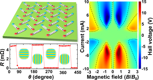 We utilize spatially reconfigurable magnetic potentials of a pinwheel artificial-spin-ice (ASI) structure to tailor the motion of superconducting vortices. The reconstituted chain structures of the magnetic charges in the pinwheel ASI and the strong interaction between magnetic charges and superconducting vortices allow significant modification of the transport properties of the underlying superconducting thin film, resulting in a reprogrammable resistance state that enables a reversible and switchable vortex Hall effect. Our results highlight an effective and simple method of using ASI as an in situ reconfigurable nanoscale energy landscape to design reprogrammable superconducting electronics, which could also be applied to the in situ control of properties and functionalities in other magnetic particle systems, such as magnetic skyrmions. We utilize spatially reconfigurable magnetic potentials of a pinwheel artificial-spin-ice (ASI) structure to tailor the motion of superconducting vortices. The reconstituted chain structures of the magnetic charges in the pinwheel ASI and the strong interaction between magnetic charges and superconducting vortices allow significant modification of the transport properties of the underlying superconducting thin film, resulting in a reprogrammable resistance state that enables a reversible and switchable vortex Hall effect. Our results highlight an effective and simple method of using ASI as an in situ reconfigurable nanoscale energy landscape to design reprogrammable superconducting electronics, which could also be applied to the in situ control of properties and functionalities in other magnetic particle systems, such as magnetic skyrmions.Nano Lett. 20 (12), 8933–8939 (2020) |
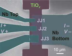
We fabricate vertical Nb/TiOx/Nb Josephson junctions where the TiOx layer is mostly metallic but has a high-resistance interface with the top Nb electrode. Thus, the junctions are in essence of the superconductor–insulator–normal-metal–superconductor type. The TiOx layer extends beyond the junction area and allows one to send an in-plane current through the normal-metal layer of the junction. We investigate and analyze dc properties (critical current, current-voltage characteristics) as well as the behavior of the junctions in external microwave fields. We find a strong dependence of all properties on the voltage Vi applied across the TiOx lead. The dependence on Vi can be mapped to the dependence of the junction parameters on the bath temperature T, when Vi is converted to an effective electronic temperature via Te=[T2+(aVi)2]1/2, with a=3.14K/mV. This relation was used before in the context of a metallic nanowire contacted by superconducting electrodes. While the geometry of our TiOx layer is far from that of a nanowire, the scaling works perfectly well for all experimental data. Our data also indicate that the electronic temperature is homogeneous throughout the junction area, a result that is unexpected for the large junction sizes we use. The device allows easy and relatively fast in situ manipulation of the junction parameters.
Phys. Rev. Applied 14, 024008 (2020)
|
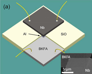
We fabricated hybrid Josephson junctions between a Ba0.5K0.5Fe2As2 (BKFA) single crystal and the conventional superconductor Nb with normal metal Al as the barrier. An in situ process was used to create clean BKFA/Al/Nb interfaces. Current transport is along the c-axis of BKFA. The current–voltage characteristics are slightly hysteretic at low temperatures. Except for some features indicative of resonant modes the shape of the current–voltage characteristics can be well described by the resistively and capacitvely shunted junction (RCSJ) model, with a product of the Josephson critical current and the normal state resistance of the junction exceeding 180 μV at low temperatures. The temperature dependence of the Josephson current is linear for temperatures down to 2 K. Under 40 GHz microwave irradiation integer Shapiro steps are observed. The power dependence of the Shapiro step-height is in good agreement with RCSJ simulations. Possible relations of our data with the symmetry of the superconducting order parameter of BKFA are discussed.Supercond. Sci. Technol. 33, 025014 (2020) |

We demonstrate an in situ fabrication technique which enables us to minimize interfacial degradation and to fabricate vertical Josephson junctions by employing few-layer BP as a barrier between two closely spaced Nb electrodes. The current–voltage characteristics of the junctions are hysteretic at low temperatures and become nonhysteretic when approaching the junction critical temperature. In the resistive state the differential conductance increases with decreasing voltage. Microwave-induced Shapiro steps were observed, confirming the presence of the ac Josephson effect. We present different models to analyze the current–voltage characteristics and conclude that resistive state of the current–voltage characteristics points to a zero bias anomaly, which is presumably caused by Andreev reflections. Our in situ fabrication technique represents a viable way to incorporate air-unstable materials for electronics and offer a chance to explore their unique functionalities.Supercond. Sci. Technol. 32, 115005 (2019) |
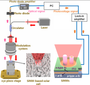
We here adopt a laser excitation photoelectric microscope (LEPM) technology to probe the local light harvesting and photoelectric signals of 3D hydrogenated amorphous silicon (a-Si:H) RJ thin film solar cells constructed over a Si nanowire (SiNW) matrix, with a high spatial resolution of 600 nm thanks to the use of a high numerical aperture objective. The LEPM scan can help to resolve clearly the impacts of local structural damages, which are invisible to optical and SEM observations. More importantly, the high-resolution photoelectric mapping establishes a straightforward link between the local 3D geometry of RJ units and their light conversion performance. Surprisingly, it is found that the maximal photoelectric signals are usually recorded in the void locations among the standing SiNW RJs, instead of the overhead positions above the RJs. This phenomenon can be well explained and reproduced by finite element simulation analysis, which highlights unambiguously the dominant contribution of inter-RJ-unit scattering against direct mode incoupling in the 3D solar cell architecture. This LEPM mapping technology and the results help to achieve a straightforward and high-resolution evaluation of the local photovoltaic responses among the 3D RJ units, providing a solid basis for further structural optimization and performance improvement.ACS Nano 13, 10359-10365 (2019) |
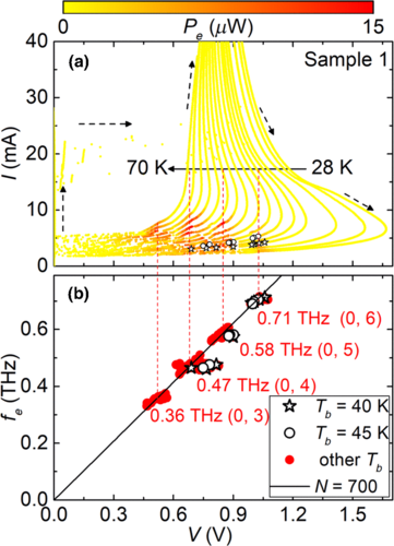
We report on a detailed investigation of terahertz-emission properties related to resonant cavity modes. We discuss data for an underdoped and an optimally doped Bi2Sr2CaCu2O8+x (BSCCO) intrinsic junction stack having the same geometry. At high bias, in the presence of a hot spot, the emission frequency seems to be continuously tunable by changing the bias current and the bath temperature. By contrast, at low bias the emission frequencies fe are remarkably discrete and temperature independent for both stacks. The values of fe point to the formation of (0,m) cavity modes with m=3 to 6. The total voltage V across the stack varies much stronger than fe, and there seems to be an excess voltage indicating groups of junctions that are unlocked. For the case of the underdoped stack we perform intensive numerical simulations based on coupled sine Gordon equations combined with heat-diffusion equations. Many overall features can be reproduced well and point to an unexpected large value of the in-plane resistivity. However, unlike in experiment, in simulations the different resonant modes strongly overlap. The reason for this discrepancy is presently unclear.Phys. Rev. Applied 11, 044004 (2019) |
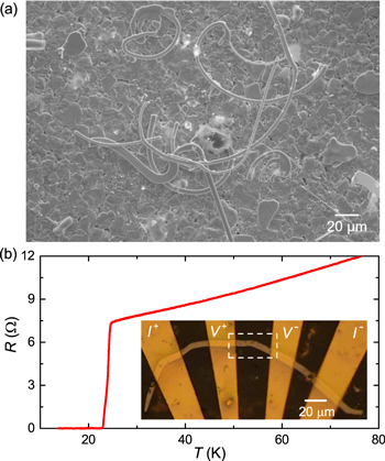
We investigated the transport properties of a curved iron-based superconducting whisker, a geometry which is considered to be interesting for electronic applications. The current–voltage characteristics (IVCs) are bi-stable at low temperatures, exhibit multiple branches at intermediate temperatures and are continuous but nonlinear at temperatures close to the superconducting transition temperature Tc. Low temperature scanning laser microscopy revealed that the multiple branches arise from a localized hot spot which for the different branches appears at different positions along the whisker. By contrast, at low temperatures Joule heating completely overheats the sample to temperatures above Tc in the resistive state. Close to Tc, the hot spot disappears and the IVCs are continuous. In the multiple-branch region, the whisker can be switched between different states by laser irradiation, provided that the laser is positioned at the location of the hot spot. The effect could be interesting for using the whisker as a photon detector or as a position-sensitive opto-electronic switch.Supercond. Sci. Technol. 32, 025010 (2019) |
We report on a Stirling-cooled compact Bi2Sr2CaCu2O8+δ intrinsic Josephson-junction stack with very high critical current density and improved cooling, operating at bath temperatures Tb up to 86 K. A record high value of 0.577 THz is obtained for the emission frequency at Tb =80 K, which is important for potential applications using liquid nitrogen as a coolant.Physical Review Applied 10, 024041 (2018) |
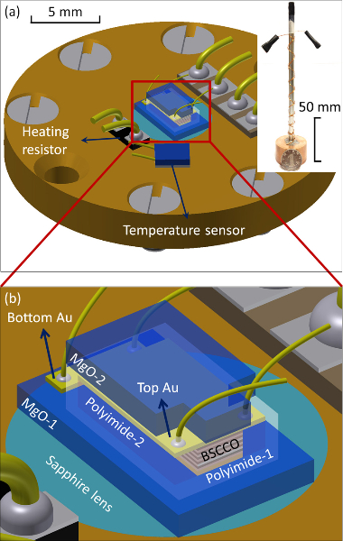
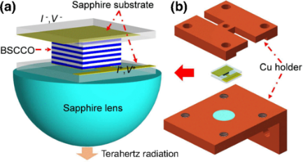
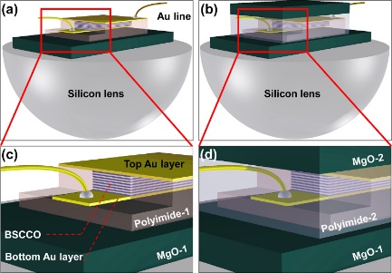
We developed a liquid-nitrogen-cooled compact source for continuous terahertz (THz) emission. The emitter is a Bi2Sr2CaCu2O8-δ intrinsic Josephson-junction stack embedded between two gold layers and sandwiched between two MgO substrates. The radiation is emitted to free space through a hollow metallic tube acting as a waveguide. This convenient and economical setup may find applications in fields like tracer-gas detection or nondestructive evaluation.Phys. Rev. Applied 3, 024006 (2015) |
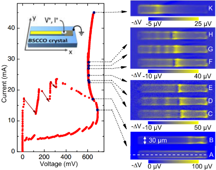
We report on the electrothermal behavior and the terahertz emission properties of a stand-alone Bi2Sr2CaCu2O8 intrinsic Josephson junction stack contacted in a three-terminal configuration. For a given total injection current, the device allows to vary the emission frequency on a 10% level by altering the injection profile. The overall tunability of the emission frequency, varying also the total bias current, is on the order of 20%.Appl. Phys. Lett. 107, 122206 (2015) |
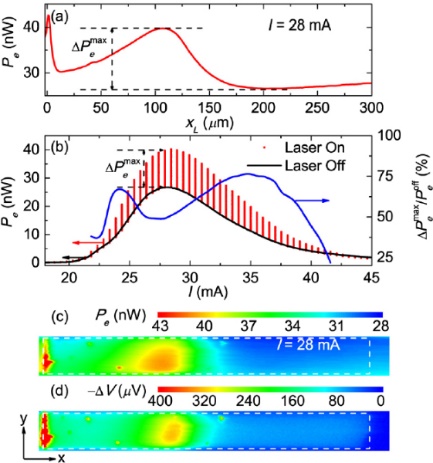
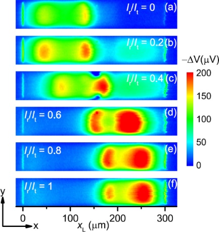
We investigated on tuning the THz emission of a Bi2Sr2CaCu2O8 (BSCCO) intrinsic Josephson-junction stack by a focused laser beam which is scanned across the stack. The emission power Pe increases by up to 75% upon laser irradiation for a bath temperature near 22 K. This tuning method can be employed in the application of BSCCO THz sources. Phys. Rev. Applied 3, 044012 (2015) |
We developed a Bi2Sr2CaCu2O8 (BSCCO) intrinsic Josephson junction stack with improved cooling, allowing for a remarkable increase in emission frequency compared to the previous designs. This double-sided cooling may also be useful for other “hot” devices, e.g., quantum cascade lasers.Appl. Phys. Lett. 105, 122602 (2014) |
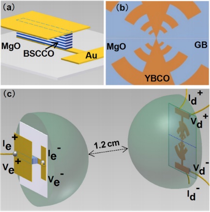
We have combined a stand-alone Bi2Sr2CaCu2O8 intrinsic Josephson junction stack, emitting terahertz radiation, with a YBa2Cu3O7 grain boundary Josephson junction acting as detector. The setup, although far from being optimized, may be considered as a first step towards an integrated high-Tc receiver.Appl. Phys. Lett. 102, 092601 (2013) |
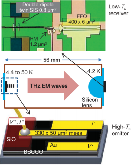
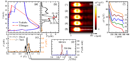
We measured the linewidth f of terahertz radiation emitted from intrinsic Josephson junction stacks, using a Nb/AlN/NbN integrated receiver for detection. While at low bias we found f to be not smaller than 500 MHz, at high bias, where a hot spot coexists with regions which are still superconducting, f turned out to be as narrow as 23 MHz. We attribute this to the hot spot acting as a synchronizing element.Phys. Rev. B 86, 060505(R) (2012) (Editors' Suggestion) |
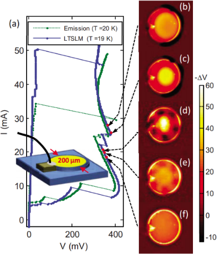
We studied on THz emission measurements and low temperature scanning laser imaging of Bi2Sr2CaCu2O8 intrinsic Josephson junction stacks. Coherent emission is observed at large dc input power, where a hot spot and a standing wave, formed in the ‘cold’ part of the stack, coexist. By changing bias current and bath temperature, the emission frequency can be varied by more than 40%.Phys. Rev. Lett. 105, 057002 (2010) |
We investigated the interplay of hot spots and standing electromagnetic waves by low-temperature scanning laser microscopy and THz emission measurements, using stacks of various geometries. The results support the picture of the hot spot acting as a reflective termination of the cavity, formed by the cold part of the mesa.Phys. Rev. B 82, 214506 (2010) |
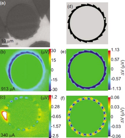
We demonstrate the operation of a deterministic fluxon ratchet made of a stack of 30 intrinsic Bi2Sr2CaCu2O8 Josephson junctions. The ratchet has the shape of a gear with 20 asymmetric teeth periods. We used low-temperature scanning laser microscopy to demonstrate that voltage rectification indeed is due to directed fluxon motion, in agreement with numerical simulations.Phys. Rev. B 80, 224507 (2009) |
Large stacks of intrinsic Josephson junctions in Bi2Sr2CaCu2O8 can emit synchronous THz radiation, the synchronization presumably triggered by a cavity resonance. To investigate this effect, we use low temperature scanning laser microscopy to image electric field distributions. We verify the appearance of cavity modes at low bias and in the high input-power regime we find that standing-wave patterns are created through interactions with a hot spot, possibly pointing to a new mode of generating synchronized radiation in intrinsic Josephson junction stacks.Phys. Rev. Lett. 102, 017006 (2009) |
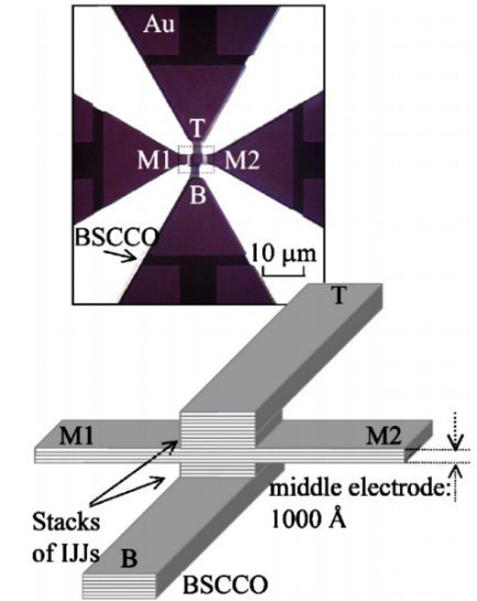
Modifying the double-sided fabrication method we invented a few years ago, a new type of Bi2Sr2CaCu2O8 intrinsic Josephson junction (IJJs) array is explored in which, in addition to the indispensable top and bottom electrodes, there is an electrode only 100 nm thick fabricated in the middle of the array. This electrode provides easy access to the inside of the IJJs, enabling us to understand the device physics better than was possible before. As the first application of such a new device, we have clearly shown how “hot” a junction stack can be under various bias conditions.Appl. Phys. Lett. 86, 023504 (2005) |

High frequency responses of intrinsic Josephson junctions up to 2.5 THz, including the observation of Shapiro steps under various conditions, are reported and discussed in this Letter. The sample was an array of intrinsic Josephson junctions singled out from inside a high Tc superconducting Bi2Sr2CaCu2O8-δ single crystal, with a bow-tie antenna integrated to it. The number of junctions in the array was controllable, the junctions were homogeneous, the distribution of applied irradiation among the junctions was even, and the junctions could synchronously respond to high frequency irradiation.Phys. Rev. Lett. 87, 107002 (2001) |


